Subject Code & Title : EEEE3098 VLSI Laboratory Simulation & Layout Software
This Laboratory forms part of the assessment for the Integrated Circuits and Systems module
EEEE3098. It must be written as a formal report and submitted via Moodle no later than This report is 30% of the overall marks for this module with the usual penalties for late submission.
EEEE3098 VLSI Laboratory – Simulation & Layout Software Assignment – UK.

Introduction :
Very Large Scale Integration design today is carried out totally by use of a computer. The Computer Aided Design (CAD) route for full custom VLSI design is typically as follows:
1.Schematic : System drawn using schematic symbols such as NAND gates, flip-flops etc.
2.High Level Simulation: System simulated either at the gate or behavioural level
3.Cell Design : Individual cells are designed and simulated at the transistor level using SPICE or a similar circuit level simulator. This is called the Pre-layout simulation
4.Cell Layout : CAD layout used to layout individual transistors in each cell”Polygon pusher”
5.Design Rule Check :The various features drawn are checked for minimum size and separation (DRC)
6.Net list Extract : Capacitance, resistance and the netlist is now extracted automatically from the layout
7.Electrical Rule Check : The circuit is now checked for electrical violations (ERC), ie outputs short circuit
8.Simulation : The circuit is now re-simulated with SPICE, with the parasitics calculated in (6) above included. This is called the Post layout simulation.
9.System Layout : Complete chip is laid out and if necessary steps 5, 6, 7 and are repeated at the system level.
10.Verification : The layout is converted either to a transistor or a gate description. This is then compared with the original schematic description in (1) above.
11.Mask Generation : The layout, usually described in a text form, is then converted into a photo mask. One of the standard text layout forms is CIF (Caltech Intermediate Format)
Computers today can handle designs with many thousands of transistors. The package being used in this exercise is freeware software.
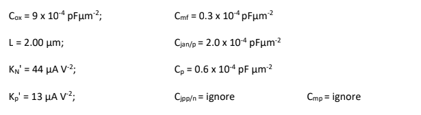
The IC process being used in this Laboratory is the silicon gate CMOS process and has the following process parameters:
Aim :
The aim of this Laboratory exercise is to:
(i) Characterise by computer simulation the transient performance of a previously designed CMOS inverter under both pre- and post-layout conditions.
(ii) Provide experience of CMOS layout structures and the associated CAD tools that are used to create and test them, as described above.
(iii) Design a CMOS NAND3 gate at the schematic level and produce a valid layout design.
Software Installation :
Two pieces of software are used for this laboratory – Lasi7 and LTspice. They are on Moodle in the archive “VLSI coursework software”. These software are available from Moodle and can be run on any Windows computer. Please install them.
Note that it is not the aim of this exercise to demonstrate the idiosyncrasies of this CAD package so I make no apologies for not explaining all the possible commands.
Part 1 – Inverter Analysis :
1.Cell Design : (Pre Layout) :
We shall assume that a CMOS inverter has been designed at the transistor level, pre-layout, such that both transistor widths and lengths are 3.5μm and 2μm, respectively. A pre-layout transistor net list description for this circuit is provided in the file inverter pre.cir in the folder VLSI_Design. Click LTspice XVII on your desktop and then open the file inverterpre.cir. Examine the file and deduce the meaning of each statement in the netlist. Then do the following and
include them in your report:
1.Check that the connectivity of the netlist is correct for a CMOS inverter. Do this by drawing the circuit diagram in your report and label the nodes of your diagram with the node numbers and component names from LTspice net list.
2. Verify that the input capacitance of 12.6fF stated in the netlist is correct for the inverter.To do this, calculate the capacitance using an appropriate equation together with the CMOS size and process parameters given in Introduction.
Note also that an output capacitance of 100.8fF has been added which represents eight similar inverters loading the output. Note: this value will be changed later on in the lab exercise. We need to run a transient analysis which will be used to record the output voltage of the inverter over time, resulting from the input waveform specified in the net list.
1. Include the transient plot to your report annotating it to indicate the discharging and charging gate delays gc and gd and record the approximate values.
Click File->Export data as text to save the transient raw data to inverterpre.txt. They can be examined with any text editor. Use them to achieve a better resolution of delay times. The pre-layout simulation for transient conditions is now complete, but before moving on:
2.Check your values of gc and gd by calculation and compare these with the results obtained from the spice simulation.
3. Inverter Layout :
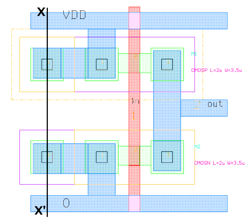
A possible layout for the inverter is presented next and is also printed at the end of this document. To start the CAD software Lasi7, run C:\Lasi7\Lasi7.exe if you installed Lasi 7 in the default folder. You may create a shortcut for Lasi7.exe on your desktop. Click Browse to select the folder VLSI_Design and then select Inverter.cir and then click OK. Click List to bring up a list of available cells. Double click on inverter and then click OK. A coloured layout should appear. Identify the two MOS transistors, the N-well, the Field Oxide etc.
EEEE3098 VLSI Laboratory Simulation & Layout Software Assignment – UK.

If the inverter layout isn’t centred in the screen properly, press “Alt f”. If the layout becomes obscured at any point you can also use “alt f” to refresh the display. If you get in a mess press the ESC key. If this doesn’t fix things then choose Undo along the top. If you still have a problem then you will need to re-copy the VLSI_Design folder.
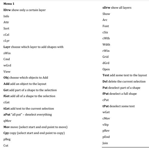
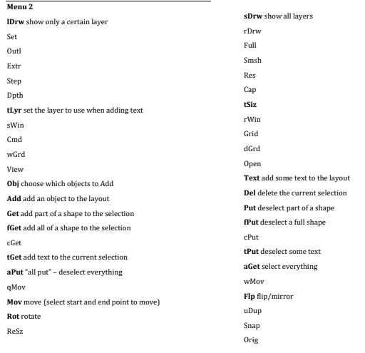
The LASI window is divided into three areas: The drawing window, which is the main area, the button bank on the right and the menu bar. The menus don’t function in the same way as normal menus do – they act as buttons instead.
There are actually two banks of buttons available on the right hand side. Clicking on “Menu 1” or “Menu 2” at the top of the bank will change banks, as will clicking the right mouse button in the drawing area. Not all of the buttons actually change function. The function of relevant buttons is explained in the page at the end of this document.
Measure the width and length of the transistor within Lasi. The values should be displayed in μm in the bottom left hand corner of the window. Clicking on the button “Grid” will add/remove a grid on the drawing area. The coarseness of the grid can be changed by clicking on “Dgrid”.
1.Write down the width and length you have measured and label them on a copy of the layout and include in your report, confirming that your value of W/L agrees with that stated earlier in this document.
3.Net list Extraction :
We now must extract a transistor netlist and parasitics present on the layout. This is carried out with “Lasi Ckt”. Click “System” in LASI and select “LasiCkt”. Check that the cell for extraction in “Setup” is “inverter” as before and select vlsi.hdr and vlsilab.drc as Header File Name and Footer File Name, respectively. Finally, at the LasiCkt7 menu click “Go” to extract the net list. Debug any errors you get – there should be none!
The net-list is contained in “inverter.cir”. Open the net-list with the LTSpice software and note the new value of input and output capacitance. Notice that the input capacitance (16.26fF) is now different from previous one because of it includes additional gate parasitics.
1.Using the process data given in Introduction, calculate values for Cin and C out including additional gate parasitics and compare them with the ones calculated by the software. Use a copy of the inverter layout to highlight the different areas you are considering to compute capacitance values.
4.Simulation of Extracted Circuit (Post-Layout Simulation)
Save “Inverter pre. cir” to “Inverter post.cir” and then update the C_in and C_out with the values from inverter.cir. The extracted net-list with parasitics, Inverterpost.cir, can now be re- simulated in LTspice.
1. Include the transient plot to your report as you did before annotating it to indicate the discharging and charging gate delays gc and gd and record the approximate values.
The delay you just computed are the inherent (unloaded) delays for this inverter cell. We now wish to observe the cell behaviour in response to 8 unit loads and then find the fan-out loading factor ’LD for this cell (see Topic 9.2 – CMOS combinatorial Design for the definition of ’ LD). To do this, modify the inverter post.cir file, set the output capacitance value C out to 15 0fF and then run again the transient analysis. The 150fF is approximately equivalent to 8 unit loads plus the inherent output capacitance, i.e.
19.6fF + 8 x 16.26fF 150fF
You will see that the output doesn’t quite reach V dd before it starts falling again, so change the clock by editing the spice netlist. In the netlist file, find the line near the top that describes V 2 via the PULSE statement. Change the 5ns to 10 ns and the 10 ns to 20 ns – this halves the clock rate. Change the transient simulation time from 10ns to 20ns and then re-run the transient analysis.
A.Include the transient plot to your report also for the loaded case. Measure the new gc and gd to a suitable accuracy.
B. As did before, compute the delays gc and gd for the post-layout inverter in both loaded and unloaded case.
C. Compare the calculated values with the one obtained in simulation and give possible reasons why the values do not fully agree. Show how improvements can be made to the simulation, calculation or both, to obtain a better agreement.
D. Determine ’LD in units of ns/pF for both L -> H and H -> L.
E. Why is the propagation delay L -> H greater than the propagation H -> L even though the transistors are of the same size?
Part 2 – NAND3 Design and Layout
The purpose of this section is to give you a different viewpoint of layout design. Rather than just analysing existing designs, as we have done in lectures, you are here to try to design your own circuit and create the corresponding layout – taking design rules into account, of course. I hope that you will get a better understanding of how the layers fit together to make devices and circuits, as well as the related skills like circuit design and design rules.
The aim is the schematic and layout design of a digital logic cell to be used as a standard cell of height 60λ. Please note that as already mentioned, the design must be free of design rule errors. You should also try to make it as compact as possible. When marking the layouts consideration will be made of the tidiness of the design. The gate you will be designing is a NAND3 (3 input NAND gate).
Schematic Design :
The specification you must meet with your design is that the worst case switching delay must be less than 2ns when driving a load of 100fF. You must design both the P and N networks intelligently, which is to say that you must ensure that the values for τgc and τgd meet the timing requirement, but that they are also not over engineered. Do not exceed the timing specification by more than a factor of 20%, i.e. your τgc and τgd values must be greater than 1.6ns, but do not need to be identical. You should calculate the width and length for each transistor.
1.In your report, draw the NAND3 circuit diagram, indicate the widths and lengths for each transistor and show your complete calculations to demonstrate your design respects the requirements.
Layout Design :
Now you have designed your circuit, you need to start drawing the layout. Run Lasi7. Instead of selecting an existing cell, type the name of your new cell and press OK. A new window will ask you to select the cell Rank. Choose 2 and press OK.
Firstly, add the stdcell_60 cell to your design. This includes a small amount of metal that shows where the Vdd and Vss lines should go. You should extend this metal in the x direction to the final width of your cell. To add the cell, click the Obj button and choose the std cell_60 cell from the list. Now click Add and click to add the cell. To change back to being able to add rectangles, click Obj and select Box, before using Add again.
You should now start to draw your gate. You can choose what layer to draw by pressing the Layr button in the button bank on the right. Once you have done this, click Add and you can then draw rectangles of that layer. Please note that the snap grid resolution is 0.5λ. Start by drawing the device and polysilicon layers, ensuring the width and length of the overlap (i.e. the gate) are correct.
Deleting a rectangle :
Click aPut to deselect everything, click fGet (full get) and click and then click again on the layout window to draw a box around one of the corners of the rectangle you wish to delete. It should turn white. Now click Del.
Resizing a rectangle :
Click on aPut to deselect everything. Now click on the Get button. Draw a box around the edge of the rectangle you wish to resize. That single edge should turn white. Now click Mov, the click at the start point of the move, move the mouse and click on the destination.
EEEE3098 VLSI Laboratory Simulation & Layout Software Assignment – UK.
Moving a rectangle :
Use Get or fGet to select the entire rectangle, then use Mov as above to move the whole rectangle.
DRC :
Once you have finished the layout of your gate you should run DRC to check it is valid. Click the System menu, then LasiDrc. In the LasiDrc window, click Setup to ensure that the cell name is correct and select vlsilab.drc from the folder VLSI_Design as DRC File Name. Next make sure that “Start check” is 1, and “Finish check” is 100. You should also always click “Fit” to ensure that the DRC tool looks at the smallest complete area possible.
Once the DRC has run (click Go), you should get a message about any errors. If you have any, you can open the DRC error map file using the Map menu from LasiDRC.
Post Layout Check :
1. After you have completed your layout, make an estimate of the output capacitance of your layout design. Your estimate should include the junction capacitance only, there is no need to add the wire capacitance. Include your calculations in your report. Does your design still meet the required timing? If not, please modify the design to meet the requirements.
2. Check also the input capacitances: does they respect the requirements?
EEEE3098 VLSI Laboratory Simulation & Layout Software Assignment – UK.

Final Steps :
After your design is complete you should include a good quality screen capture (not photograph!) of the complete design in your report. You should also create a zip of the VLSI_Design folder and submit that alongside your report, so that I can verify the files myself. Please note that missing design files will result in lost marks, so take care to include all of the files you have produced.
Report guidelines :
Report must not exceed 10 pages. Please use Microsoft Word or an equivalent software to write it, including equations. Do not put hand-written parts. Also schematic and diagram have to be drawn with a software of your chose.
The usual deduction will apply for work submitted late. Do not leave your submission to the last minute, even a few seconds late will incur the late penalty.Draft submissions will not be accepted as a final submission. If you make a draft submission on time and mark it as final after the deadline, you will incur a late penalty.Plagiarism and collusion are actively checked for. Please do not allow anyone else access to your work, even your friends.
ORDER This EEEE3098 VLSI Laboratory Simulation & Layout Software Assignment NOW And Get Instant Discount

Read More :-
COCS71198 A Proposal For Virtualisation Within Excel Ltd Assignment 1 – UK.

