Module Title: Digital Electronic Design Automation
Module Number: EN0720/KD7020
Weighting (to overall module): 60%
Learning Outcomes tested in this assessment (from the Module Descriptor):1.Appreciate the need for, and understand the use of system-level design languages such as System-Verilog.
2.Create and implement Register Transfer Level (RTL) designs from system-level specifications, by use of design methodologies, such as Algorithmic State Machines and implement designs using programmable hardware.
3.Develop their knowledge, skill, and resource and time management applied to advanced design tools and languages in an independent manner.
EN0720/KD7020 Digital Electronic Design Automation Assignment-Northumbria University UK
Assessment Criteria/Mark Scheme:
See Assignment Script
Nature of the submission required:
Word document (3000-5000 words approximately)
Instructions to students:
Referencing Style:
All referencing should be in Harvard style.
Academic Conduct:
You must adhere to the university regulations on academic conduct. Formal inquiry proceedings will be instigated if there is any suspicion of misconduct or plagiarism in your work. Refer to the University’s regulations on assessment if you are unclear as to the meaning of these terms. The latest copy is available on the university website.
Objectives:
- To create System Verilog (SV) design source descriptions for the various component parts of a Monitoring System comprising an Analogue-to-Digital Converter, Asynchronous Serial Data Transmitter and Receiver along with a display.
- To incorporate an IP (Intellectual Property) module into the design using customisation and interfacing.
- To perform simulations of individual design modules using SV test-modules and the Vivado® Simulator.
- To perform simulations of the complete Monitoring System top-level module using a SV test-module and the Vivado® Simulator.
- Synthesise and Implement the Monitoring System, targeting a Field Programmable Gate Array development board (Artix-7 FPGA on Digilent® Basys3® development board).
- Demonstrate the operation of the FPGA implementation of the Monitoring System using the Basys3® development board by means of a so-called ‘hardwired loop-back’ test.
Learning Outcomes:
See Assignment Specification document:
‘EN0720_KD7020_assignment_2020_21_Specification_part1.docx’.
Supporting Documentation (available on eLearning portal)
- Power point presentation on Register Transfer Level Design using the System Verilog hardware description language. See document on e Learning: ‘RTL with System Verilog
- Workshop exercise on ‘XADC’ built-in Analogue-to-Digital Converter (Workshop 4), see document: ‘XADC_Display_SV_2019.pdf’
Assignment 1 – Description of the Monitoring System
Figure 1, below, shows a simplified block diagram of the Monitoring System and figure 2 shows the corresponding physical layout of the Basys 3 development board.
EN0720/KD7020 Digital Electronic Design Automation Assignment-Northumbria University UK
The system is driven by a 100 MHz crystal clock and an active-high reset push button, when the latter is pressed, the entire system is reset. The main functional blocks that make up the system are shown in figure 1:
i. XADC – built-in Analogue-to-Digital Converter that can be instantiated from the IP library. The analogue input voltage range is 0.0 to +1.0 Volts.
ii. XADC Controller – responds to manual or timer generated pulses initiating an ADC conversion, it produces the required control signals for the XADC and interfaces with the transmitter.
iii. Transmitter – after each conversion, the 12-bit result is transmitted over an asynchronous serial data link as an individual character.
iv. Receiver – receives the asynchronous character from the transmitter and displays the value on the 7-segment display.
This assignment involves the design, verification and implementation of the Monitoring System using a Field Programmable Gate Array (FPGA) device, this is achieved through a series of guided tasks.
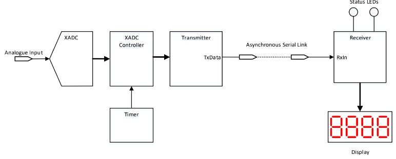
Figure 1 – Simplified block diagram of the Monitoring System
The physical layout of the Monitoring System implemented using the Digilent® ‘Basys3’ development board, shown in figure 2, illustrates the location of the main inputs and outputs.
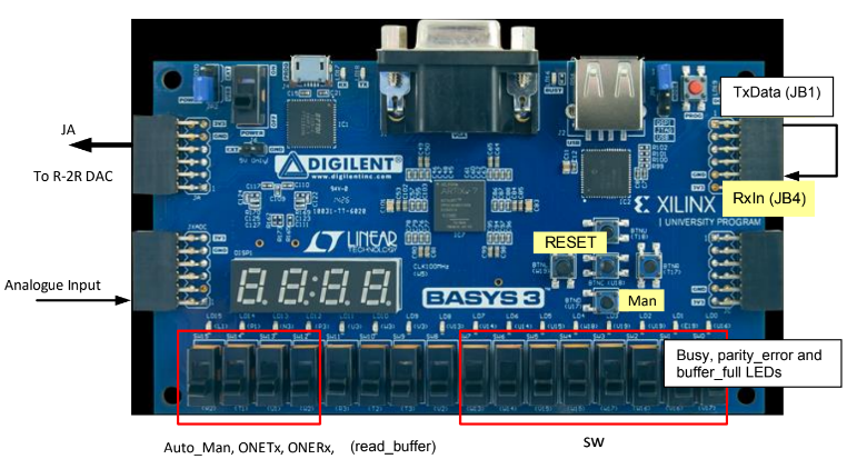
Figure 2 – Physical layout of the Monitoring System on Basys 3 Board
Figure 3, below, is a more detailed internal block diagram of the Monitoring System. The shaded blocks shown in figure 3 are implemented within the Artix-7 FPGA device. The 4-digit, 7-segment display, R-2R ladder network Digital-to-Analogue Converter, clock generator and various buttons
and switches are located on the Basys3 board and connected to specific FPGA pins as specified in the ‘*.xdc’ (Xilinx Design Constraint) file.
Figures 3a and 3b show the left- and right-hand sides of the system in more detail.
Figures 3 (3a and 3b) shows the FPGA pin designators next to each input/output terminal, for example, the transmitter output ‘TxData’ is allocated FPGA pin ‘A14’, and this in turn is connected to header connector ‘JB1’, as shown in figure 2.
The R-2R DAC, shown at the top left-hand corner of figure 3, is an external plug-in ‘PMOD’ module. This is used to produce a test voltage for input to the XADC, the value of which is set by the eight sliding switches ‘SW0..7’. When testing the Basys 3 board it is important to ensure the switches are set such that the test voltage is within the range of the XADC unipolar input, i.e. 0.0 to +1.0 Volts.
Careful study of all three figures (3, 3a and 3b) will reveal that interconnecting signal names and module port names have been matched throughout the design (see red box in figure 3a), with one or two exceptions. This allows the use of the System Verilog automatic port connection feature, considerably shortening and simplifying the source descriptions.
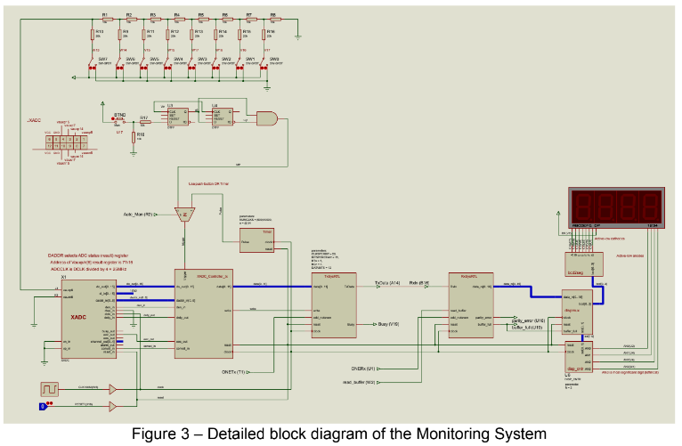
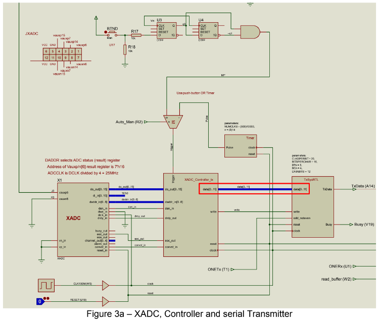
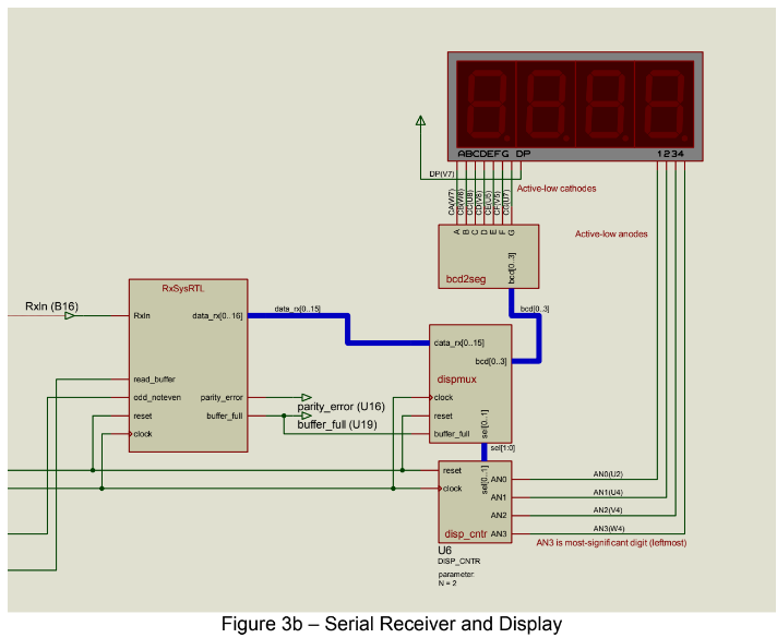
Figure 4 shows the timing format for the characters being transmitted by the ‘TxSysRTL’ module,(transmitter) on the serial data output ‘Tx Data’, and received by the ‘Rx Sys RTL’ (receiver) block on the serial data input ‘Rx In’.
The most-significant 12-bits of each 16-bit result from the A-to-D converter is embedded within a data character having a start-bit, parity-bit (odd or even) and one or more stop-bits, in the same manner as a UART (Universal Asynchronous Receiver-Transmitter).
To allow synchronisation between transmitter and receiver, each individual serial bit has a duration set by the ‘CLKSPERBIT’ parameter. In between data character transmissions, the serial communication line remains high.
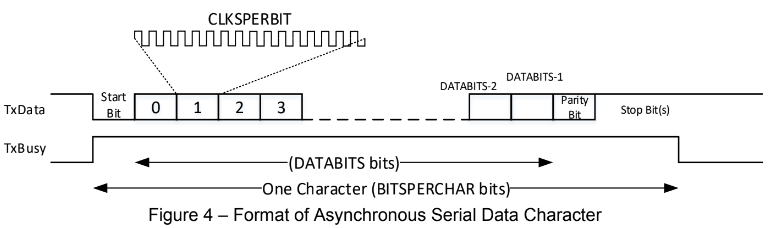
The transmitter also outputs a ‘Tx Busy’ signals which goes high at the falling edge of the start-bit and returns to logic-0 at the end of the last stop-bit (after ‘BITSPERCHAR’ bits). This signal can be used to prevent a transmitting data source from attempting to send data prior to the end of the current transmission. The ‘DATA BITS’ parameter sets the number of data bits in the character,and this along with the other two parameters shown in figure 4 are common (but independently set) to both the transmitter and receiver.
EN0720/KD7020 Digital Electronic Design Automation Assignment-Northumbria University UK
The serial transmission of ADC data values can be controlled in the following ways, the first two of these are provided for by the circuitry shown in figures 3, 3 a and 3 b:
i. Automatic conversion and transmission at intervals set by the Timer module. With the ‘Auto_Man’ input set to logic-1, the XADC ‘trigger’ input (triggers a conversion) receives pulses from the Timer module at intervals set by the Timer parameter ‘NUMCLKS’ (number of 100 MHz clock pulses).
ii. Manual conversion and transmission invoked by the ‘Man’ push button. Pressing ‘BTND’ on the Basys 3 board produces one ‘trigger’ pulse, this feature is enabled when the ‘Auto_Man’ input set to logic-0.
iii. Maximum conversion and transmission rate determined by XADC conversion time and time to transmit one data character. In this mode, data characters are transmitted continuously with the start-bit immediately following the last stop-bit of adjacent characters.
Task 1 – Create a SV source description of the ‘RxSysRTL’ module
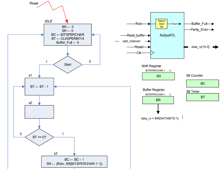
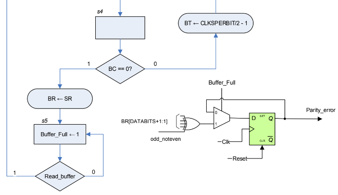
Figure 5 shows the ASM chart and other details relating to the receiver module ‘RxSysRTL’.
The figure shows the behaviour of the module in the form of an ASM chart, along with a symbolic representation and the main internal registers. The internal signal named ‘Start’ is derived from the serial data input ‘Rx In’ such that a single clock-pulse-length pulse is produced on ‘Start’ each time
‘RxIn’ undergoes a logic-1 to logic-0 transition (Refer to figure 3, the ‘MP’ circuit plays a similar role).
At the bottom right hand corner of figure 5, a logic circuit is included to illustrate the operation of the ‘Parity’ error output (parity_error). The system enters state ‘s5’ once a complete serial data character has been received (the shift register (SR) is transferred to the buffer register (BR) in the previous state, ‘s4’) and a logic-1 is transferred to the ‘buffer_full’ output. The ‘buffer_full’ signal enables the parity circuit flip-flop to load a value from the respective logic shown on the diagram(Exclusive-OR and Nand gate).
In the event of a parity error, the ‘parity_error’ output flag remains high until, either a master reset occurs, or the next data character is received
The parallel data output of the receiver module ‘data_rx’ is 16-bits in length, in order to drive the 4- digit hexadecimal display logic directly. The data value received from the transmitter occupies the lower bits of this output bus.
The receiver cannot receive another serial data character until the buffer is read, i.e. the‘read_buffer’ input is asserted.
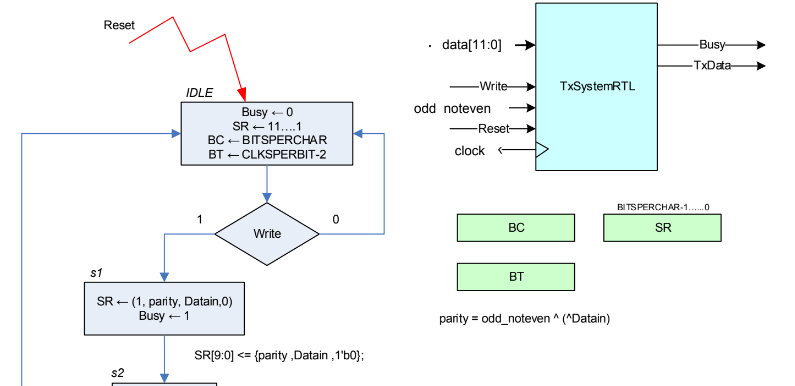
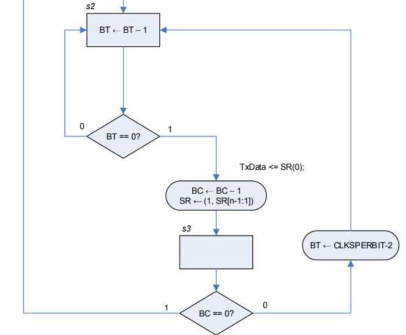
Appendix A contains a listing for the transmitter module ‘TxSysRTL’, in the form of a System Verilog register transfer level (RTL) description. Appendix B contains the corresponding ASM chart for the transmitter.
Using the information provided in appendices A and B, along with figure 5, create a complete Register Transfer Level (RTL) SV source description for the receiver module, saving it in a text file named ‘RxSysRTL.sv’. The receiver module is to have an identical set of parameter declarations
when compared to the transmitter module. The source file can be created within the Xilinx Vivado® software, alternatively Notepad++ could be used.
Include a full listing of the ‘RxSysRTL’ module in your report, presented in a style consistent with that used in Appendix A (consolas font, reserved words bold, comments in italics with appropriate use of indentation). Do not use a screen-copy of the listing as it appears within the Vivado text editor.
Task 2 – Complete the test-module provided in Appendix A and verify the correct operation of the Transmitter and Receiver modules
Having created the SV source description for the receiver in task 1, this can be combined with the transmitter module in order to verify correct operation. The source description for the transmitter module is provided in Appendix A – ‘TxSysRTL.sv’.
Figure 6 shows a block diagram of the incomplete test-module provided in Appendix A, named ‘test_TxRxSysRTL’.
Note that the diagram below shows an 8-bit ‘data’ port for the purposes of simulation only.
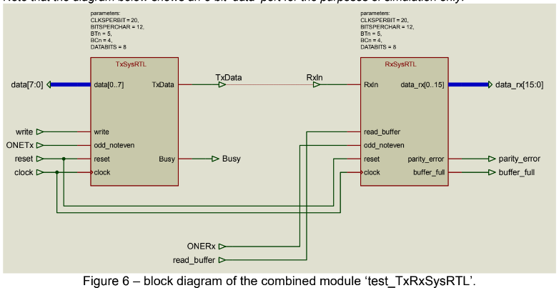
The SV source listing for the test-module (‘test_TxRxSysRTL.sv’) provided in Appendix A requires the addition of module-instantiation-statements and a continuous-assignment statement, with the parameters of the instantiated transmitter and receiver modules set to the values shown in figure 6.
Include a full listing of the ‘test_TxRxSysRTL.sv’ module source in your report, presented in a style similar to that used in Appendix A (consol as font, reserved words bold, comments in italics with appropriate use of indentation). Highlight the statements you have added as detailed above.
Do not use a screen-copy of the listing as it appears within the Vivado text editor.
Use the Xilinx Vivado FPGA design software to create a new RTL project for this assignment,targeting the device on the Digilent Basys3 development board.
Add the SV sources, provided and created so far, to the project. Ensure that any simulation test- modules are added/created as ‘simulation’ sources.
The project should contain the following sources:
‘Tx Sys RTL.sv’ (see Appendix A)
‘RxSysRTL.sv’ (Task 1)
‘test_TxRxSysRTL.sv’ (Task 2 – see Appendix A)
Perform a behavioural simulation of the top-level simulation test-module (test_TxRxSysRTL), after the simulation has initially run for 1 us, add the following internal signals to the wave window, restart the simulation and rerun until the ‘$stop’ command is executed in the test-module.
Transmitter: TxState, BT and BC.
Receiver: RxState, BT, BC and Start.
Capture and paste an image of the full extent of the simulation wave forms into your report,ensuring all top-level and added internal signal names are legible at the left-hand side. Add a suitable caption to the image and comment on the results.
EN0720/KD7020 Digital Electronic Design Automation Assignment-Northumbria University UK
Zoom in to the wave forms in order to enclose a single data character (between two consecutive‘write’ pulses).
Capture and paste an image of the single character waveforms into your report, ensuring all top-
level and added internal signal names are legible at the left-hand side. Add a suitable caption to
the image. Confirm that the data value appearing at the ‘data_rx’ port, coincident with the assertion of the ‘buffer_full’ receiver output, matches the value applied to the ‘data’ port of the transmitter, during the ‘write’ operation.Pan across the wave forms to check that each value transmitted is correctly received by the ‘Rx Sys RTL’ module correctly.
Zoom in to the wave forms to enclose an individual data bit (1 or 0). The values of the internal states and counters should be readable (set radix to unsigned decimal for the latter). Place the cursor on the waveform to show at what point the receiver shift register is loaded with the value present on ‘Rx In’.
Capture and paste an image of the wave forms into your report, ensuring all top-level and added internal signal names are legible at the left-hand side. Add a suitable caption to the image.Measure the width of the data-bit using the cursors and markers in the wave window, comment on the value recorded.
Modify the source descriptions of the test-module and/or DUT to demonstrate the correct behaviour of the ‘parity_error’ output of the receiver. Capture appropriate wave forms and document the changes made to the sources. Briefly explain the operation of the parity error circuit.
Task 3 – Add the remaining sources to the Vivado RTL project
Go to the e Learning portal and locate the ‘XADC Display (SV)’ item in the ‘Week 4’ folder of module KD7020(EN0720), as shown in the image below.

Download both the PDF and ZIP file onto your student-drive and extract all files from the archive into your Viva do project folder.
Compare the diagram on page 1 of the file ‘XADC_Display_SV_2019.pdf’ with figure 3 above, it is evident that some of the source files are common to both designs:
- XADC_Controller.sv – requires modification, rename the file and module as ‘XADC_Controller_tx’.
- Timer.sv – identical
- bcd2seg.sv – identical
- DispCntr.sv – identical
- DispMux.sv – replace with provided source.
- testbench.sv – requires modification, no need to change the file and module name.
- Basys3_XADC_RTL.xdc – requires modification, rename the file as ‘Basys 3_XADC_Tx Sys_Rx Sys_Display. xdc’
- XADC_RTL_Display.sv – requires modification, rename the file and module as ‘XADC_Tx Sys_RxSys_Display’. This is the top-level design source.
Prior to adding the above files to your Viva do project, rename those source files indicated above, the required changes to the source descriptions can be made after the files have been added to the project. All source files, apart from ‘test bench.sv’ are for both simulation and implementation (i.e. design sources), whereas ‘test bench’ is for simulation only.
The ‘XADC’ IP module, instantiated within the top-level design, must be regenerated by means of the ‘IP Catalog’ in the Flow Navigator, by following the procedure described in the document ‘XADC_Display_SV_2019.pdf’.
Once all files have been added to the project, and the XADC module regenerated and embedded into the top-level module, capture an image of the ‘Sources’ window from within the PROJECT MANAGER. It may be necessary to float the panel out in order to view the entire design and
simulation hierarchy. Note that the design hierarchy view will depend upon whether or not the required modifications to the source files have been made, therefore this image should be captured once the changes carried out in Task 4 have been made.
Task 4.1 – Modify the ‘XADC_Controller_tx’ module
Page 28 of the ‘XADC_Display_SV_2019.pdf’ document shows the existing ASM chart for the control block ‘XADC_Controller’. As shown in figure 3 (3a) above, an additional output, named ‘write’, is required to drive the ‘write’ input of the transmitter module ‘TxSysRTL’.
The ‘write’ signal is to be asserted during an additional state named ‘TRANS’ that is entered unconditionally from the ‘GET_DATA’ state. Note that ‘write’ is a direct output that occurs during state ‘TRANS’, it is not a register transfer.
The added state ‘TRANS’ leads unconditionally back to the ‘WT_TRIG’ state.
Figure 3a also shows an additional modification of the ‘XADC_Controller_tx’ is required. The ‘data’output port is 12-bits rather than 16-bits wide. In the ‘GET_DATA’ state, the most-significant 12- bits of the XADC output data (do_out) is to be transferred to the ‘data’ output register.
Draw a modified ASM chart for the ‘XADC_Controller_tx’ module, showing the additional state and modified register transfer described above. Include a copy of the modified ASM chart in your report.
Include a full listing of the modified ‘XADC_Controller_tx.sv’ module source in your report,presented in a style similar to that used in Appendix A and highlighting the changes you have made (consol as font, reserved words bold, comments in italics with appropriate use of indentation). Do not use a screen-copy of the listing as it appears within the Viva do text editor.
EN0720/KD7020 Digital Electronic Design Automation Assignment-Northumbria University UK
Task 4.2 – Complete the top-level design module source description ‘XADC_TxSys_RxSys_Display.sv’.
Compare figure 3 on page 4 of this document (XADC_TxSys_RxSys_Display) with the diagram on page 2 of the ‘XADC_Display_SV_2019.pdf’ document (XADC_RTL_Display). The major difference between the two systems is the addition of the bit-serial transmitter and receiver modules to the design.
Study figure 3 carefully and make the necessary modifications to the SV source file ‘XADC_TxSys_RxSys_Display.sv’, adding the extra input/output ports and internal signals associated with the communications channel along with the instantiations of the ‘TxSysRTL’ and ‘RxSysRTL’ modules. Add a continuous assignment to describe the multiplexer that selects between the timer-generated and manual trigger pulses (‘Auto_Man’ input). Make use of the SV automatic port connection feature in order to shorten and simplify the net-list.
Include a full listing of the modified ‘XADC_TxSys_RxSys_Display.sv’ module source in your report, presented in a style similar to that used in Appendix A (consolas font, reserved words bold, comments in italics with appropriate use of indentation). Do not use a screen-copy of the listing as it appears within the Viva do text editor.
Task 5 – Modify the simulation test-module source file ‘testbench.sv’.
The Verilog-HDL test-module imported from the ‘XADC_Display_SV_2019’ project requires modification for use with the top-level module developed in Task 4.2.
The main changes are as follows:
i. Add identically named declarations of input and output signals for the ‘TxSysRTL’ and ‘RxSysRTL’ modules along with the ‘Auto_Man’ selection input (use type logic).
ii. Add a continuous assignment to connect the transmitter output to the receiver input,‘TxOut’ to ‘RxIn’, thereby creating the ‘loop-back’ test.
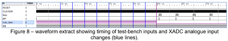
iii. Add sequential statements to the initial block shown below, to create the stimulus required to show correct automatic and manual transmission across the link, using the waveform extract shown in figure 8.
Include a full listing of the modified ‘test bench.sv’ module source in your report, presented in a style similar to that used in Appendix A (consolas font, reserved words bold, comments in italics with appropriate use of indentation). Do not use a screen-copy of the listing as it appears within
the Vivado text editor.
Task 6 – Create the XADC analogue input stimulus file, ‘design.txt’, and perform a functional simulation of the top-level design module using the ‘test bench’ module.
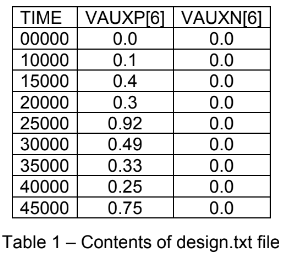
Table 1 shows the values and times for the simulated analogue voltages applied to the vaux[6] input channel.
The values change at intervals of 5us (apart from the first change to 0.1), this matches the ‘Timer’parameter ‘NUMCLKS’, which is set to 500 for simulation.
Copy the contents of Table 1 in order to create the ‘design.txt’ stimulus file. Note that this text file is used during the configuration of the XADC IP block.
Run a Behavioural Simulation of the top-level simulation test-module. Add the following signals to the Wave window in the vertical order shown (delete any signals that are not in the list):
Set the radix of any bus signals appropriately, usually hexadecimal, and change colours to attempt to make the wave forms more readable.
Capture a number of alternative views of the wave forms (full, zoomed-in etc.) and add them to your assignment document with captions and comments. Use the wave forms to confirm correct operation of all parts of the system, from the timer triggering a conversion of the analogue in out ,
to the display of the equivalent digital value in hexadecimal format on the 4-digit display.
Task 7 – Complete the Design Constraints file‘Basys 3_XADC_Tx Sys_RxSys_Display.xdc’, implement the design and configure the Basys 3 FPGA Board
After renaming the existing Xilinx Design Constraint file ‘Basys3_XADC_RTL.xdc’, as ‘Basys3_XADC_TxSys_RxSys_Display.xdc’, and adding it to the project, edit the file so that all top-level inputs and outputs are associated with the correct physical FPGA pin numbers.
Refer to figure 3 for details of all pin numbers, these are shown in parentheses ‘( )’ next to each port name.
EN0720/KD7020 Digital Electronic Design Automation Assignment-Northumbria University UK
Some of the pins used in the top-level design module are already included in the constraint file (for example, the display pins). Those that are missing must be un commented and edited, see below for an example:
Include a listing in your report of the contents of the completed
‘Basys3_XADC_TxSys_RxSys_Display.xdc’, file. Unused FPGA pins may be deleted in order to shorten the listing, highlight the changes/additions required for the present design.
Change any module instance parameters to those that are compatible with implementation (Timer and Display Counter). Copy the changes into your assignment report and comment.
Run the Viva do Implementation process and capture a screen image to show successful implementation.
Generate the Bit-stream file and use the Hardware Manager to configure the Basys 3 FPGA board.
Capture images showing correct operation of the system using your smartphone (you can measure the analogue input voltage using a DVM if available).There may be an opportunity to do a practical demonstration of the design in the laboratory. Try connected two Basys3 boards together and transmit from one to the other.
EN0720/KD7020 Digital Electronic Design Automation Assignment-Northumbria University UK
TxSysRTL ASM Chart
ORDER This EN0720/KD7020 Digital Electronic Design Automation Assignment NOW And Get Instant Discount